

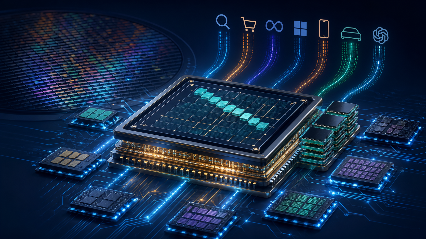
For most of the modern AI era, the hardware story sounded simple. NVIDIA built the accelerators. Everyone else bought them, assembled clusters around them, and tried to get in line before supply ran out.
That story is now obsolete.
The most important new entrants in AI silicon are not traditional merchant chip vendors. They are cloud platforms, consumer-device companies, and frontier AI labs: Google, Amazon, Meta, Microsoft, Apple, Tesla, and now OpenAI. Some of these companies have been designing internal AI silicon for years. Others are newer to the effort. What unites them is not a shared chip design, but a shared conclusion: at large enough scale, a general-purpose GPU is no longer the only economically rational way to train models, serve inference, or reserve future supply.
This shift matters because it changes both the market structure and the engineering assumptions underneath it. The next phase of AI infrastructure will not be defined by one company winning every workload. It will be defined by specialization. NVIDIA still owns the broadest software ecosystem and the most complete merchant platform. But around that platform, a growing number of companies are carving out custom silicon for recommendation engines, large language model inference, sparse retrieval, edge inference, privacy-sensitive on-device AI, and tightly controlled internal training environments.
The technical nuance is the important part. These chips are not all attempting to become “another GPU.” In most cases, they are doing the opposite. They are trading away some generality in exchange for better locality, lower latency, lower power, simpler scaling for a specific workload, or a supply chain that depends less on the most contested components of the AI boom.
The Real Reason Non-Chip Companies Are Building Chips
The first driver is economics. Merchant GPUs are expensive not only because the silicon is advanced, but because buyers are paying for a broadly programmable machine with a mature software moat, high-bandwidth packaging, a scale-up fabric, and a vendor margin layered over all of it. That is a strong value proposition when your workloads are mixed, your models change rapidly, or your developers need a stable abstraction. It becomes less attractive when you are running the same few classes of models at hyperscale every day.
That is why custom silicon keeps showing up first in highly repetitive workloads. Meta’s MTIA program started in recommendation inference, where the company could tailor the hardware to ranking models, embedding-heavy data flows, and PyTorch execution patterns it understands intimately. OpenAI’s Jalapeno effort is inference-oriented rather than a blank-check attempt to replace every accelerator in its fleet. Microsoft has pushed Maia toward large-scale inference. AWS split its strategy across Trainium for training and Inferentia for inference, each exposed through the Neuron stack. The point is not ideological independence. The point is shaving cost and wasted motion out of a workload whose behavior is now predictable enough to specialize.
The second driver is supply control. “Owning the chip” does not mean owning the fab, but it does mean controlling the package shape, the memory strategy, the deployment cadence, and the software contract above the silicon. In an environment where leading-edge wafers, high-bandwidth memory (HBM), CoWoS-class advanced packaging, and even substrate capacity remain contested, that control matters almost as much as peak TOPS.
The third driver is power. AI datacenters are increasingly constrained by megawatts, not just accelerators. A chip that delivers meaningfully better performance per watt for a narrow workload can change whether a service fits inside an existing power envelope or requires a new rack, a new liquid-cooling design, or a new utility negotiation. That helps explain why so many custom architectures obsess over data movement. Arithmetic is cheap compared with shipping tensors back and forth across the memory hierarchy.
The fourth driver is platform leverage. Custom silicon is also a way to bind software, deployment, and infrastructure together. Google can make TPUs more attractive when XLA, JAX, pod topology, and cloud deployment are all designed to fit the hardware. AWS can do the same with Neuron. Microsoft can do it with Maia and Azure’s inference stack. Even Apple, though it is not selling a datacenter accelerator, is doing a version of this with the Neural Engine, GPU-side neural accelerators, unified memory, and Private Cloud Compute running on Apple silicon.
None of this means merchant GPUs are going away. It means the market now has enough scale that large buyers no longer want to outsource every hardware decision to the merchant market.
The New Entrants Are Not All Entering for the Same Reason
One way to flatten this story into nonsense is to talk about “hyperscalers building chips” as if they are all doing the same thing. They are not. The list of entrants matters precisely because each company is targeting a different problem.
Google is the veteran here. TPUs are no longer an experiment or a sidecar coprocessor. They are a mature in-house platform with their own execution model, software path, and pod-scale deployment assumptions. In the source research, the more recent TPU generations continue Google’s long bias toward systolic matrix engines, large-scale interconnect, and compiler-shaped execution through XLA. Google is not entering the space so much as proving that internal AI silicon can become a durable product category rather than a one-off infrastructure hedge.
Amazon’s approach is different. Trainium and Inferentia are part of AWS’s attempt to expose custom silicon as a first-party cloud primitive. That means the hardware has to be technically specialized while still behaving like rentable infrastructure rather than an internal-only curiosity. The Neuron software stack matters here as much as the silicon itself, because AWS is not just optimizing for its own workloads. It is trying to make those workloads portable enough that customers will accept the migration friction in exchange for better economics.
Meta’s motivation is more tightly internal. MTIA has been publicly framed around recommendation systems first, then broader GenAI inference. That distinction matters. Recommendation inference is not the same problem as frontier model training, and Meta’s public design choices reflect that. The early generations leaned into large on-chip SRAM, LPDDR rather than HBM, and a processing-element mesh that better fits ranking and retrieval-style workloads. Later roadmap disclosures move harder toward GenAI inference, but the design philosophy still begins with Meta’s own production traffic, not the merchant market.
Microsoft’s Maia program sits somewhere between AWS and Meta. Maia is not sold like a merchant accelerator, but it also is not just a private science project. It exists to support Azure’s AI platform economics and to reduce dependence on a purely external accelerator roadmap. Public material emphasizes inference, memory-system design, and scale-up networking rather than a fully exposed alternative programming universe. That makes sense. Microsoft does not necessarily need Maia to become the industry’s favorite chip. It needs Maia to become strategically useful inside Azure.
OpenAI is the most symbolically important new entrant because it is not historically thought of as a chip company at all. Jalapeno matters less for what is publicly disclosed about the die and more for what its existence signals: a frontier model lab now sees direct silicon involvement as part of infrastructure strategy. Publicly, the chip is framed around large language model inference, memory movement, networking, and serving behavior rather than a universal training-and-inference answer. That is exactly what you would expect from a company trying to reduce dependence on merchant inference supply without pretending it suddenly needs to out-NVIDIA NVIDIA.
Apple and Tesla round out the picture in ways that prove the category is broader than cloud AI alone. Apple’s AI hardware strategy is about vertical integration across device silicon, runtime, and privacy-preserving server extension. Tesla’s Dojo program is a training-oriented system built around its own autonomy workloads and topology assumptions. Neither company is entering the market to become a general merchant chip vendor. Both are building silicon because their workloads are important enough, and weird enough, that owning the hardware contract creates leverage.
That is the common thread across the entrants. They are not entering because chip design became fashionable. They are entering because the scale, repetition, and strategic value of their workloads became too important to leave entirely to merchant supply.
Most Custom AI Chips Are Not Trying to Be Better GPUs
The easiest way to misunderstand this market is to assume every new AI chip is a head-to-head attack on NVIDIA’s architecture. That is usually false.
NVIDIA’s core advantage is not just raw throughput. It is the combination of a general-purpose single-instruction, multiple-thread (SIMT) execution model, Tensor Cores for dense math, NVLink and NVSwitch for scale-up, and the immense maturity of CUDA, PTX, NCCL, TensorRT, and the rest of the software ecosystem. GPUs are messy-workload machines. They are designed to stay useful even when kernels are irregular, operator mixes change, model code is ugly, and developers want to move quickly.
Most custom accelerators narrow that target on purpose.
Google’s TPU line is the clearest historical example. TPUs are built around systolic matrix engines, not a SIMT programming model. In the newer generations described in the source research, Google continues leaning into large matrix units, explicit compiler guidance through XLA, and enormous pod-scale fabrics. That makes TPUs extremely strong when the workload can be compiled and tiled cleanly into the hardware’s favored execution shape. It also means performance depends more heavily on layout discipline and compiler behavior than many GPU users are accustomed to.
AWS Trainium and Inferentia sit at a different point in the design space. Rather than looking like stripped-down GPUs, they expose heterogeneous engines per core: tensor, vector, scalar, and general-purpose SIMD, coordinated with explicit on-chip buffers such as SBUF and PSUM. That sounds subtle until you think about what it implies. A larger fraction of performance comes from compiler scheduling, overlap of different engines, and careful management of scratchpad locality, rather than from a deep hardware-managed cache hierarchy dynamically hiding mistakes.
Meta’s MTIA line diverges further. Public material on MTIA v2/2i describes an 8x8 grid of processing elements, RISC-V control, fixed-function units for matrix math and nonlinear operations, plus hardware support for decompression and dynamic quantization. That is not a general-purpose GPU in disguise. It is a recommendation and inference machine designed to spend silicon area on the behaviors Meta actually sees in production.
Microsoft’s Maia approach, at least from what is public, appears less centered on exposing a novel programming model and more on system-level co-design for inference: memory subsystem choices, scale-up bandwidth, and an Ethernet-based networking strategy that lets Azure build large clusters without copying NVIDIA’s proprietary interconnect model directly. OpenAI’s Jalapeno, similarly, is described publicly as an inference-first chip optimized around kernels, memory movement, networking, and serving patterns, while many low-level microarchitectural details remain undisclosed.
Then there are the specialists that break even harder from the GPU template.
Groq’s architecture emphasizes deterministic, statically scheduled inference. Cerebras removes conventional package-level scale-up by making the processor wafer-scale. SambaNova centers execution around spatial dataflow. d-Matrix moves toward digital in-memory compute to reduce dependence on external high-bandwidth memory. Hailo optimizes for edge power envelopes rather than datacenter flexibility. These are not just different products. They are different answers to the question of where the overhead really lives in AI computation.
The Memory Hierarchy Is Where the Architectural Differences Become Real
Once you look past peak FLOPS tables, the deepest differences among these chips usually show up in the memory system.
GPUs traditionally assume a layered hierarchy of registers, shared memory, caches, and HBM. That hierarchy is powerful because it supports generality. It is also expensive in area, power, and control complexity. If your workload is regular enough, there are often better options.
That is why so many custom chips either increase on-chip SRAM aggressively or make locality visible to software.
Meta’s MTIA v2/2i is a good example. Public disclosures point to 256 MB of on-chip SRAM with roughly 2.7 TB/s of bandwidth, paired with LPDDR5 rather than HBM. That looks conservative if you are thinking in terms of maximum headline bandwidth. It looks shrewd if your workload is recommendation inference, where the hardware can exploit local reuse, decompression, and quantization support while avoiding both the cost and supply pressure of HBM-centric packaging.
AWS makes a different trade. Trainium and Inferentia still embrace HBM, but the architecture exposes local buffers and heterogeneous execution resources that push the compiler to manage movement explicitly. The hardware is acknowledging a brutal truth about AI performance: the arithmetic units are often waiting on data, so the machine should be built around staging and reusing data deliberately rather than pretending the cache will rescue every access pattern.
Google’s newer TPU generations remain firmly in the HBM camp, especially at pod scale, but the memory hierarchy is still more domain-shaped than GPU-shaped. The MXU-centric compute model rewards workloads that can be fed as large, predictable matrix streams. Google’s software story through XLA exists partly because the hardware contract is stricter.
Cerebras goes to the other extreme. The wafer-scale processor effectively inverts the normal assumption that large working sets must live off chip. Its architecture pushes a striking amount of SRAM directly onto the wafer and uses on-wafer bandwidth to reduce the need for package-level scale-up. That is a radical answer to the memory wall: if package boundaries and off-chip communication are the problem, erase as many of those boundaries as possible.
d-Matrix is solving a related problem from a different angle. By using digital in-memory compute and integrated performance memory rather than building around HBM on CoWoS, it is not simply chasing lower power. It is also routing around one of the most supply-constrained parts of modern AI manufacturing. That is a recurring theme in this market: memory architecture is now inseparable from procurement strategy.
The comparison is easier to see in a compact snapshot:
| Platform | Primary architectural bias | Memory strategy | What that says about the workload |
|---|---|---|---|
| NVIDIA Blackwell | Broadly programmable SIMT GPU | Large HBM3e pool plus cache hierarchy | Mixed, evolving workloads where flexibility is worth the overhead |
| Google TPU | Systolic matrix engine | Heavy HBM use at pod scale | Dense matrix-heavy training and inference with compiler-managed layouts |
| AWS Trainium | Heterogeneous engines plus scratchpads | HBM plus explicit local buffers | High-throughput cloud workloads where compiler control can recover efficiency |
| Meta MTIA | PE mesh with RISC-V control and fixed-function units | Large SRAM plus LPDDR, not HBM in v2/2i | Recommendation and inference paths with predictable locality and tight cost targets |
| Cerebras WSE | Wafer-scale compute fabric | Massive on-wafer SRAM, no conventional HBM-centric model | Large models where communication overhead is the enemy |
| d-Matrix Corsair | Digital in-memory inference | Integrated performance memory plus off-chip capacity memory | Interactive inference where moving weights efficiently matters more than generality |
This is why vague claims that one chip is “faster than NVIDIA” are usually useless. Faster at what precision? With what model shape? Under what memory-access pattern? Using whose compiler? The answer changes constantly, because these chips are optimized for different bottlenecks.
The execution-model differences become even clearer if you line up the major designs side by side.
Google’s TPU family is fundamentally matrix-centric. The research points repeatedly to systolic MXU-style execution and XLA-shaped software flows. That gives Google a machine that is extremely good at dense matrix work when the compiler can tile it cleanly, but it also means efficiency depends on respecting the hardware’s preferred dataflow.
AWS takes a more heterogeneous path. Rather than centering everything around one kind of execution unit, Trainium and Inferentia expose tensor, vector, scalar, and general-purpose SIMD engines plus explicit local buffers and communication structures. The burden shifts toward compiler scheduling and data placement. That is less elegant to describe than “it’s another tensor accelerator,” but it is closer to what the hardware is actually doing.
Meta’s MTIA line is more visibly workload-shaped. Public material around v2/2i describes an 8x8 mesh of processing elements, dual RISC-V control inside those elements, and fixed-function support for things like matrix operations, nonlinear functions, decompression, and dynamic quantization. The architecture is not trying to disappear into a generic abstraction. It is trying to match the behavior of the recommendation and inference jobs Meta actually runs.
Groq, Cerebras, and d-Matrix each break a different GPU assumption. Groq tries to eliminate a large amount of runtime uncertainty through deterministic static scheduling. Cerebras attacks the communication problem by making the processor wafer-scale rather than accepting a package-and-cluster model as inevitable. d-Matrix attacks the memory wall by moving compute closer to memory and reducing dependence on HBM-heavy packaging. Put differently, the differences are not cosmetic. Each vendor is choosing a different place to spend complexity.
Packaging, Interconnect, and HBM Have Become Part of the Architecture
Ten years ago, many software people could treat packaging as backend manufacturing trivia. That luxury is gone.
Modern AI accelerators are no longer just dies. They are multi-die systems assembled through 2.5D or 3D packaging, bound tightly to HBM stacks, interposers, substrates, reticle limits, and test capacity. In practical terms, the package now determines how much memory bandwidth the software can see, how many chiplets can be integrated economically, how much power can be delivered, and whether the product can ship in meaningful volume at all.
That is why TSMC’s CoWoS capacity, HBM allocation from SK hynix, Samsung, and Micron, and advanced backend assembly keep showing up in strategic conversations. The leading-edge logic node still matters, but many of the current bottlenecks sit downstream of the wafer.
The architectural consequences are visible everywhere.
Google scales TPUs with its own interconnect fabric and very large pod designs. Microsoft is publicly leaning on standard Ethernet with custom transport rather than a direct NVLink clone. AWS scales through successive NeuronLink generations and larger server-level domains. Tesla’s Dojo exposes a locality-aware 2D mesh and makes the topology visible to software. Groq treats deterministic multi-chip coordination as part of the architecture itself. The interconnect is no longer a box outside the accelerator. It is part of the accelerator’s design thesis.
Packaging decisions are also producing different forms of specialization.
Some vendors, including the hyperscalers building large training or inference clusters, still embrace HBM-heavy advanced packages because the workload simply demands it. Others are trying to escape the worst bottlenecks. Meta’s choice to use LPDDR for MTIA v2/2i in recommendation inference is one example. Cerebras’ wafer-scale design is another. d-Matrix’s use of organic-substrate chiplets and non-HBM memory hierarchy is another still. These are not secondary implementation details. They are market strategy expressed through physical design.
This is also where “custom silicon” stops meaning only the compute die. The serious programs are co-designing silicon, package, board, rack, cooling, and fabric as one system. That is why Broadcom, Marvell-like design partnerships, foundry relationships, and system integrators remain so important. The firms that ship successfully are not merely writing RTL. They are reserving packaging slots, securing memory, planning board bring-up, and aligning compiler assumptions with the machine that actually lands in the rack.
The Manufacturing Bottleneck Has Moved Downstream
The attached research is especially strong on one point that gets missed in a lot of AI chip coverage: leading-edge logic is no longer the only bottleneck, and in some cases it is not even the immediate one.
The modern AI accelerator is produced through a layered ecosystem. Most of the companies now designing custom AI silicon are fabless. They own the workload definitions, architectural choices, physical design priorities, compiler stack, and system integration plan, but they do not own wafer fabrication. They rely on foundries for advanced logic, memory vendors for HBM, advanced-packaging providers and OSATs for assembly and test, and EDA/IP vendors to keep the entire program from collapsing under its own complexity. That means “in-house silicon” is more accurately described as orchestrated silicon.
This is why TSMC’s CoWoS capacity keeps appearing next to HBM shortages and ASML lead times in the same conversation. The bottleneck has moved downstream from the die itself into the combination of memory, packaging, substrates, and backend assembly. A company can finish the RTL and still not have a meaningful product if it cannot secure HBM allocation, advanced package capacity, board-level validation throughput, and enough manufacturing slack to survive a respin.
The source research makes that supply-chain coupling explicit. HBM shortages are not just procurement headaches; they shape architecture. CoWoS pressure is not just an operations problem; it changes which package styles are even realistic. Test and assembly are not afterthoughts; they determine when a chip becomes deployable infrastructure rather than a celebrated tape-out announcement.
That is why some architectural choices now read like supply-chain strategy in disguise. Meta’s SRAM-plus-LPDDR approach in MTIA v2/2i is not merely a microarchitectural curiosity. It also reduces dependence on the most contested HBM-heavy package flows. Cerebras’ wafer-scale design is not just radical engineering theater. It is another path around some of the scale-up and multi-package constraints that dominate more conventional systems. d-Matrix’s avoidance of HBM-centric CoWoS packaging makes the same argument from a different angle.
The timeline implications matter too. In the research, tape-out is only one phase. After that come packaging reservations, HBM procurement, test, validation, system integration, and cluster bring-up. That is why new AI silicon programs can no longer be understood as chip-design stories alone. They are program-management stories spanning design, supply, packaging, and deployment all at once.
This is also where the non-traditional entrants gain and lose leverage. They can reduce dependence on NVIDIA by designing their own accelerators. They cannot reduce dependence on the semiconductor ecosystem as a whole. The dependency is redistributed, not eliminated. Instead of buying a finished merchant platform, they now manage a web of dependencies across foundries, HBM vendors, packaging houses, OSATs, system integrators, and software tooling. That is a harder game, but at hyperscale it can still be the rational one.
What Changes in the Market From Here
The AI chip market is not moving toward a simple NVIDIA-versus-someone-else showdown. It is moving toward a stacked market.
At the top of that stack, NVIDIA likely remains dominant in merchant accelerators for the foreseeable future. The reasons are familiar: CUDA is still the most important software moat in AI infrastructure, NVLink-scale systems remain powerful, and GPUs are still the safest answer when workload diversity, developer productivity, and ecosystem maturity matter more than squeezing every last watt or dollar out of a narrow problem.
Beneath that, hyperscalers and frontier AI labs will keep building internal “workload islands” where specialization pays off. Recommendation serving is one island. LLM inference is another. Embedding and retrieval-heavy systems are another. Privacy-sensitive on-device AI is another. In each case, the goal is not to replace the entire accelerator fleet. The goal is to own the workloads where the company has enough volume, enough software control, and enough predictability to justify custom silicon.
Below that layer, specialist startups will survive where they can prove a structural advantage rather than a marketing one. Groq’s value proposition is low-latency deterministic inference. Cerebras’ is eliminating conventional scale-up pain. d-Matrix is betting that memory movement and HBM avoidance matter enough to justify a very different inference architecture. Hailo wins where edge power constraints dominate. These companies do not need to beat NVIDIA across the board. They need to own one painful corner of the trade space.
This fragmentation will make the market harder to read with old vendor categories. “GPU company,” “cloud company,” and “AI lab” are no longer cleanly separate categories. Google is a cloud provider with a long-running silicon program. AWS is both. Microsoft is now both. Apple is a device company with a vertically integrated AI hardware stack. OpenAI is now an AI lab with custom inference silicon. In the next few years, the meaningful distinctions will be less about corporate label and more about what layer of the stack each company is trying to control.
The other major consequence is that manufacturing strategy becomes competitive strategy. The winners will not be determined only by architecture diagrams or benchmark charts. They will be determined by who can secure HBM, book packaging, keep yields under control, ship systems on time, and align the compiler with the actual deployment environment. In other words, the AI chip race increasingly looks like a supply-chain-and-systems contest disguised as a compute contest.
The Market Is Getting More Heterogeneous, Not Less
The cleanest forecast from the current wave of custom silicon is that the AI hardware market is becoming more heterogeneous.
That heterogeneity is not a temporary detour on the way back to one universal accelerator. It is the logical consequence of AI workloads becoming too large, too power-hungry, and too economically important to serve with one architectural template alone. When the workload is messy, evolving, and broad, the GPU still wins. When the workload is stable enough that the overhead can be designed out, custom silicon becomes attractive fast.
That is the deeper meaning of so many non-traditional entrants moving into chip design. They are not doing it because building advanced silicon suddenly became easy. It has not. They are doing it because the scale of modern AI has made the old buy-only model strategically incomplete.
So the right mental model for the next phase of AI hardware is not “Which chip replaces the GPU?” It is “Which parts of the stack are now valuable enough for companies to own directly?”
For Google, the answer includes pod-scale matrix engines. For AWS, it includes training and inference ASICs tied to Neuron. For Meta, it includes recommendation and GenAI inference hardware matched to internal workloads. For Microsoft, it includes an inference-first Azure substrate. For Apple, it includes on-device and private-cloud vertical integration. For OpenAI, it now includes internal inference silicon designed around its own serving patterns.
And for NVIDIA, the answer remains what it has been all along: sell the most generally useful high-end compute platform in the market, then force everyone else to justify every departure from it.
That is a much more interesting market than the one AI infrastructure had a few years ago. It is also a more technically demanding one. The companies entering custom silicon are no longer just buying compute. They are choosing execution models, memory hierarchies, packaging strategies, and supply-chain dependencies as first-class business decisions. Once that happens, the chip is no longer just a component. It becomes the operating doctrine of the platform built around it.